
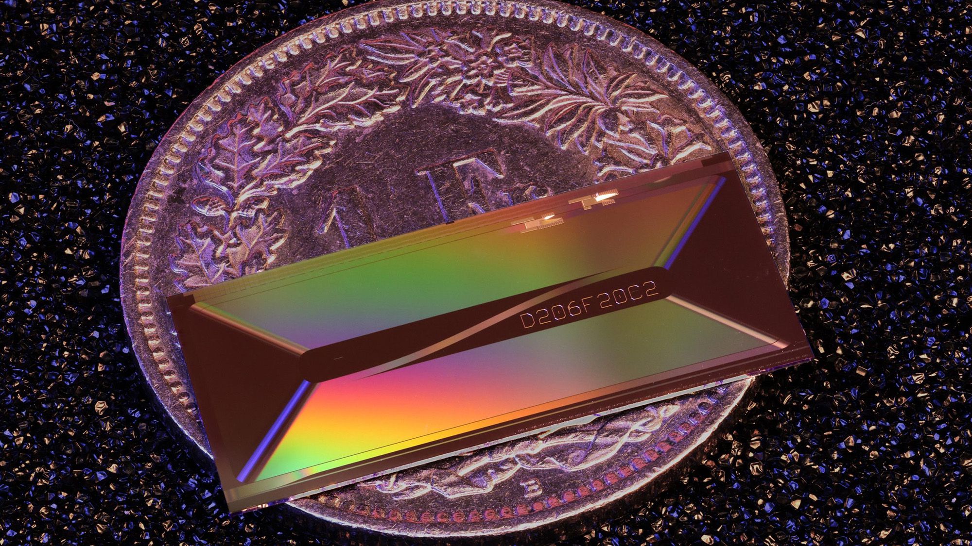
A breakthrough in photonic chips could make large, costly, ultrafast lasers dramatically smaller, leading to portable and affordable imaging, diagnostic and information-processing devices, researchers say.
By using a decades-old overlooked laser architecture, scientists managed to fit an ultrafast laser onto a tiny photonic chip — a chip that uses light, rather than electricity, for computing operations.
In a new study published June 3 in the journal Nature, the team demonstrated that a tiny laser on the photonic chip could deliver 1.05 nanojoules of energy in 147-femtosecond (147 quadrillionths of a second) bursts — thereby competing with the output of laboratory-class ultrafast lasers.
Ultrafast lasers are used in a variety of applications, from precision manufacturing and eye surgery to biological imaging and atomic clocks, but the systems needed to power them tend to take up whole tabletops in labs or factories. Yet the powerful output of these laser pulses made them difficult to miniaturise onto photonic chips.
“For more than twenty years, a high-pulse-energy femtosecond laser on chip was widely regarded as a holy grail of integrated photonics,” Tobias Kippenberg, a photonics professor at the Swiss Federal Institute of Technology(EPFL), said in a statement.
“Our result shows that it is not only possible, but that it can be achieved with a surprisingly elegant architecture that the integrated-photonics community had overlooked.”
Forward-thinking breakthrough comes from looking back
Photonic chips manipulate light by using microscopic structures called waveguides — usually in the form of optical fibers or etched cavities — to carry information. They aren’t particularly novel, and can be found in fiber-optic communications, medical sensors and lidar systems.
Get the world’s most fascinating discoveries delivered straight to your inbox.
But photonic chips have previously struggled when handling high-powered, ultrafast lasers. That’s because they need to contain light to extremely small waveguides, leading the light to interact strongly with itself and destabilizing the laser pulses.
To tackle this problem, the researchers looked at a laser architecture called the Mamyshev oscillator, created in 1998 by Pavel V. Mamyshev, a physicist and engineer at Bell Labs.

EPFL’s chip-based ultrafast laser operates in a testing set up.
(Image credit: Zheru Qiu/EPFL)
This oscillator, which has received little attention in the world of photonic chips, works by placing a nonlinear waveguide between two optical filters. This causes a high-intensity laser pulse to expand into a broader range of colors that can then pass through both filters while weaker light, which can cause laser destabilization, is blocked out. This technique essentially means that a high-intensity laser pulse can be maintained.
Because the Mamyshev oscillator doesn’t require extra components to manufacture on a chip, it presents an attractive design for use on photonic chips. And although the laser cavity needed to direct an ultrafast laser is 16.5 inches (42 centimeters) long, it can be folded to occupy around the same area as a match head. This can’t be done with conventional fiber-optic-based lasers, often used in photonic chips.
That takes care of the size, but the cost of ultrafast laser systems is another challenge. But because photonic chips can be fabricated using silicon wafers in the same fashion as computer chips, more than 1,000 laser cavities could potentially be produced in a single batch, the researchers said. As such, photonic chips with ultrafast laser capabilities could be produced at scale, in turn reducing manufacturing costs and even expanding their use.
Photonic chips capable of handling ultrafast lasers could, in the future, lead to portable tools for tasks like detecting pollutants or performing advanced medical diagnostics in the field, the researchers noted in the study. The technology also opens the door to smaller atomic clocks that can benefit navigation and future communications.
Qiu, Z., Yang, X., Li, X., Hu, J., Liu, Z., Zhang, Y., Ji, X., Sun, J., Lihachev, G., Li, Z., Kentsch, U., & Kippenberg, T. J. (2026). High-pulse-energy integrated mode-locked laser using a Mamyshev oscillator. Nature, 654(8117), 57–63. https://doi.org/10.1038/s41586-026-10517-4
